


Physical analysis
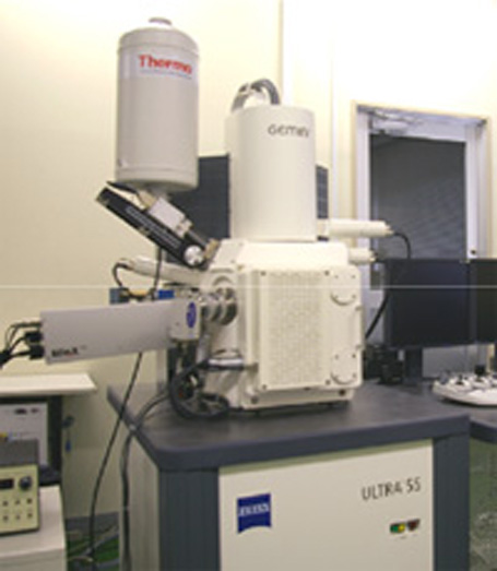
Ultra-Low Accelerating Voltage SEM (ULV-SEM)
Newly added EBSP function to Ultra-Low Voltage SEM!
Ultra-low accelerating voltage SEM £ULTRA 55¤ from ZEISS provides a new method for your problem solution and material development by state-of-the-art technology!
Features of Ultra-Low Accelerating Voltage FE-SEM
- Features 1 Observation at ultra-low accelerating voltage from 100 V is perfect for electrode surface observation.
- Features 2 Non-processing (without conductive deposition) observation of all kinds of sample including insulated object is possible.
- Features 3 High-resolution element distribution can be obtained by means of in-lens reflection electron detector (EsB)
- Features 4 The spatial resolution in EDX analysis is approx. 30 nm, smaller by two digits than the conventional spatial resolution.
- Features 5 The new EBSP allows measurement at a space solution of 100 nm or less, greater than that of conventional machine, and at a high speed.
Basic Specifications
| Electron gun | Shcottoky-type FE electron gun |
|---|---|
| Accelerating voltage | 100 V to 30 kV |
| Sample size, maximum | φ 200 mm |
| Resolution | 1.0 nm@15 kV 1.7 nm@1 kV 4.0 nm@100 V |
| Magnification | 12X to 300,000X |
| Analysis function | EDX: NSS300 from Thermo ELECTRON EBSP: Hikari High Speed EBSD Detector by EDAX (TSL) |
Past Observation/Analysis Cases at JFE-TEC
| Field | Case |
|---|---|
| Electronics/ electrics |
Lamination film structure in electronic devices (identification of flaw) |
| Section observation and EDX analysis of wire bonding portion | |
| Morphological observation of photoresist | |
| Surface contamination of wafer | |
| Observation of Pb-free mounted component | |
| Observation of magnetic material/piezoelectric element and dielectric material/fluorescent material | |
| Section observation of super lattice structure of compound semiconductor | |
| Step observation of surface of compound semiconductor | |
| Thin film/surface treatment | Section observation of functional thin film (metal, semiconductor, inorganic material, polymer) |
| Observation of morphology/roughness of film surface | |
| Observation of metallic thin film on polymer substrate | |
| Section observation of surface treatment material: observation of film internal structure and fine structure of film/substrate interface | |
| Observation/analysis of section of multilayer optical glass | |
| EBSP measurement of crystalline orientation distribution in Cu plating | |
| Observation of writing part of optical disc recording layer | |
| EBSP of writing part of optical disc recording layer | |
| Surface observation of DLC film | |
| Metal/steel | Observation of non-metallic precipitate and (composite) inclusion in metal/steel |
| Observation of intermetallic compound (submicron size or smaller) | |
| Surface oxide distribution in steel material | |
| Observation of dissimilar metal joining interface | |
| Microscopic structure observation of fracture surface and sliding surface | |
| EBSP measurement of residual austenitic phase distribution in steel material | |
| Corrosion | Section fine structure observation/EDX analysis of corrosion product in steel material |
| Observation of fine corrosion product (submicron size) in thin film surface | |
| Observation of metal surface oxide | |
| Ceramics | Observation/analysis of different oxide crystalline particles (interface) |
| Roughness observation of ceramics surface in nm level | |
| Morphological observation of ceramics fine particles (varying sizes from nm level to µm level) | |
| Section observation of functional glass | |
| Structure observation of concrete, slag and oxide potassium fertilizer | |
| High polymer | Surface observation of engineering plastics |
| Observation of additive for rubber | |
| Carbon material | Observation of CNT |
| Catalyst | Morphological observation and element distribution of various catalysts (metal, oxide, etc.) |
| Paper making | Observation of pulp and surface coating layer |
| Drug, living body, and others | Observation of addition state of inorganics and organics |
Observation Case 1: Observation of Organic Substance Attached on Si Wafer at Ultra-Low Accelerating Voltage
-
Observation of organic substance attached on Si wafer was conducted at an ultra-low accelerating voltage (100 V) without any deposition. It was found that the surface of the organic substance was not even and had many undulations. In addition, it was found that around the large organic substance at the center, small particles of approx. 100 nm in size existed on the whole plane.
In a conventional SEM condition (15 kV), the surface shape is hardly seen. At 1 kV, shape observation is difficult due to charge up.
-
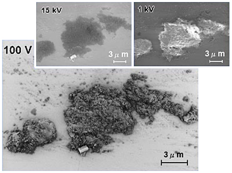
Observation of organic substance attached on Si wafer at ultra-low accelerating voltage
Sample processing: None, accelerating voltage: 100 V
Observation Case 2: Observation of Aluminum Electrolytic Capacitor at Ultra-Low Accelerating Voltage
-
It is recognized that in an anodically oxidized aluminum electrolytic capacitor, alumina (dark contrast portion) is formed on the surface of metallic Al (bright contrast portion). High magnification observation reveals grow of alumina in a columnar crystal shape.
This observation was also conducted without any deposition.
Sample offered by: NEC -
Observation of aluminum electrolytic capacitor at ultra-low accelerating voltage (Al anodically oxidized film)
Sample processing: None, accelerating voltage: 1.25 kV
Observation Case 3: Observation of Commercially Available Optical Discs
-
Observation of commercially available DVD-RW having gone through laser writing was conducted. As the surface of the recording layer was observed by using in-lens SE detector with no processing, it was found that the contrast of the portions that had been irradiated with laser and turned into amorphous were different from the surrounding crystalline portions. From this difference in contrast, it is possible to identify the recorded portions.
-
Observation of surface of recording layer of
commercially-available DVD-RW
Accelerating voltage: 400 V
Observation Case 4: Analysis of Wire Bonding Portion Using EDS
By decreasing the accelerating voltage while the electron beam diameter is small, the spatial resolution of EDS analysis has been decreased by one to two digits or more from conventional approx. 10 µm to approx. 30 nm, making it possible to analyze submicron area. In the section of a wire bonding portion as shown in the figure, Au and Al films as well as W thin film of approx. 100 nm in thickness are clearly analyzed. Also, Si and W, whose peaks overlaps with each other, can be separated by spectral mapping.
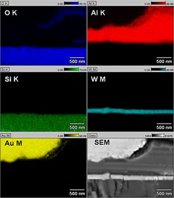
Accelerating voltage: 4 kV
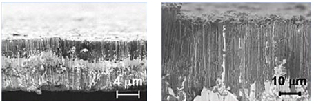
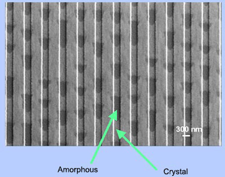
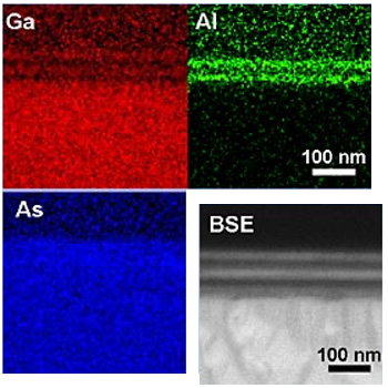
Observation Case 5: Analysis of GaAs/AlAs Super Lattice Thin Film Using EDS
In an analysis case of GaAs/AlAs superlatice thin film section, 25 nm GaAs layer and AlAs layer could be separately analyzed.
Observation Case 6: Ultra-Low Accelerating Voltage SEM-EBSP Analysis: Crystalline Orientation Mapping on the Basis of Cu Plating Crystalline Particle
Due to combination with ultra-low accelerating voltage SEM, high resolution measurement by EBSP has been made possible.
Crystalline orientation mapping of Cu plating structure in submicron size has been obtained.
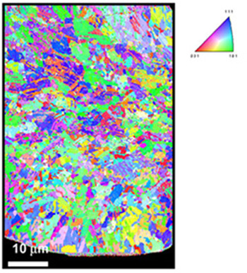
Display mode: EBSP crystalline orientation mapping
Observation Case 7: Ultra-Low Accelerating Voltage SEM-EBSP Analysis: Distribution of Residual Austenitic Phase In Steel
-
Conventionally, EBSP analysis of residual austenitic phase (γ-Fe phase) in martensite was difficult because austenitic phase is small in size and there are many distortions in martensitic phase. Due to combination with ultra-low accelerating voltage SEM, the spatial resolution of EBSP measurement has been improved and therefore distribution of residual austenitic phase in micron size has been obtained.
-
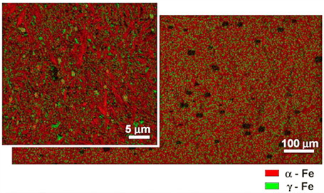
Distribution of austenitic phase in steel
Display mode: EBSP phase distribution image
Observation Case 8: Ultra-Low Accelerating Voltage SEM-EBSP Analysis: Analysis of Recording Part of Commercially Available DVD Recording Layer
Also in EBSP analysis of thin film of recording layer of commercially-available DVD (approx. 10 nm) in combination of ultra-low accelerating voltage SEM, the recorded part (amorphous phase) in submicron level and unrecorded part (crystalline phase) could be distinguished from each other.
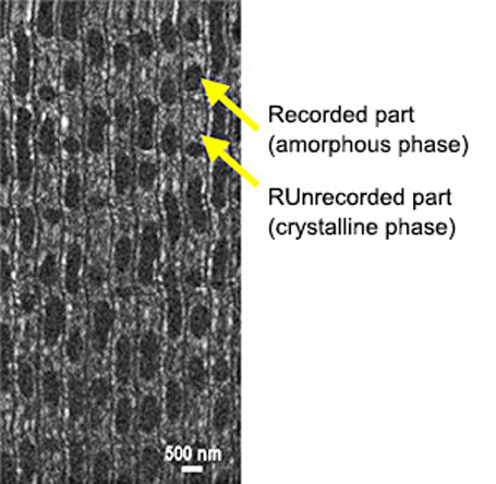
Unrecorded part (crystalline phase)
Observation of recording layer of commercially available DVD
Display mode: image quality image, accelerating voltage: 8 kV