


Total Solutions
Analysis and Investigation of Electronic Components/Electronic Devices
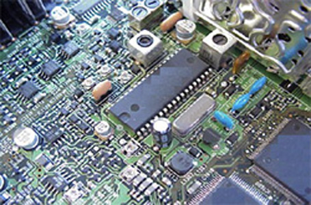
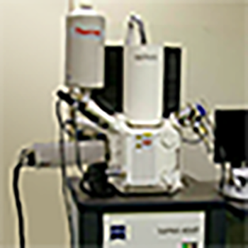
Outline of Analysis and Investigation of Electronic Components/Electronic Devices
-
To support the development of SiC and other next-generation power devices, JFE-TEC performs analyses of wafers and investigations of the microstructure of chip structures and modules.
We also perform commissioned investigations of the causes of trouble/malfunctions of LSI products, individual electronic components, mount boards and electronic parts, contributing to improvement of quality control and higher efficiency in product development by the client, as well as improved product yield. Utilizing know-how backed up by an impressive track record, we meet the client's problem-solving needs with efficient investigation and a quick response.
As part of the changeover to lead-free products of the solder alloy, we also respond quickly and accurately in evaluations of the reliability of soldered joints and similar needs.
-
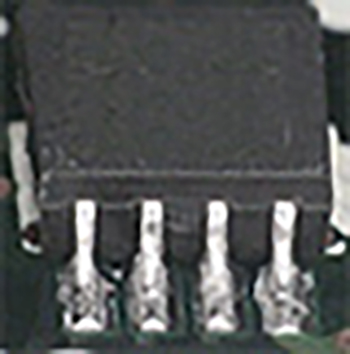
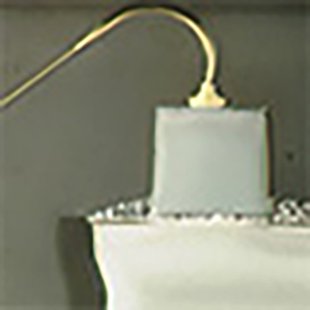
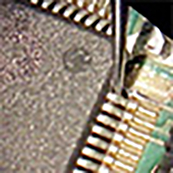
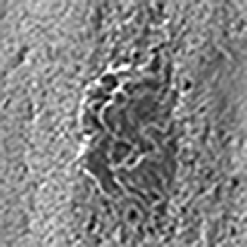
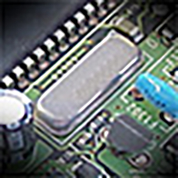
(No relation between photograph
and nonconforming phenomenon)
Industrial Fields where JFE-TEC has a Record of Accident Cause Investigation/ Analysis
- Automobiles (harnesses, control devices, motor parts, power units, etc.)
- Aircraft, electronics, household appliances, daily necessities, industrial machinery, medical equipment, security parts, etc.
Power Device Evaluation Items
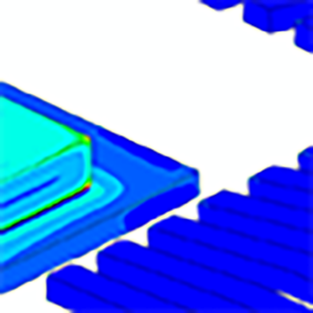
JFE-TEC conducts impurity analyses for defect evaluation of SiC wafers and epilayers, microstructural analysis of devices and analysis of mounted modules.
Examples of Main Test Items for Electronic Components/Devices
Environmental Tests (Reliability Tests)
-
- Thermal shock test
- Constant temperature/constant humidity test
- Electrostatic Discharge (ESD) resistance test
-
- Pressure cooker test
- Low temperature storage test
- Electromigration test
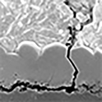
Reliability Tests of Soldered Joints
-
- Durability test
- Wettability test
- Reflow heat resistance test
-
- Peel strength test
- Bonding-wire pull shear test
Nondestructive Tests
-
- Transmission X-ray observation
- X-ray analysis microscopy measurement
-
- Ultrasonic flaw detection
- Identification of short circuit location by liquid crystal method
Test Pretreatment for Analysis
-
- FIB method
- Wire saw cutting
- Package dismantling
-
- Dicing cutting
- Precision polishing to 20 μm (approx.)
- Delamination of LSI layers
Evaluation of Electrical Characteristics
-
- Volume resistivity measurement
- V-I characteristics
-
- Measurement of interlayer electrical resistance
Examples of Investigation of Electronic Components and Printed Circuit Board Mounted Components
-
-
-
-

-
-
- Examples of Defects of Connectors
-
- Pore corrosion of Au plating
- Fretting of Sn plating
- Galvanic corrosion
-
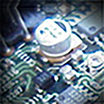
- Electrolytic Condensers
-
- Electrolyte leakage
- Valve opening
-
- Examples of Defects of Printed Circuit Boards
-
- Through-hole and wiring defects
- Black pad phenomenon
- Uncured solder resists
-
- Quartz Resonators
-
- Electrode connection defects
- Resonator destruction
Element Technologies of Electronic Component/Device Analysis and Investigation Solutions
-
- Material Testing
-
Tensile/shear strength testing under micro-load, bending endurance test
-
- Nondestructive Testing
-
Detection of hot spots by infrared camera, etc.
-

- Investigation/Analysis of Cause of Defects
-
Investigation/analysis of causes of defects of electronic components and devices
-
- Weatherability Evaluation
-
Weather meter test, atmospheric exposure test
-
- Physical Analysis
-
Element mapping, SIM/SEM observation, etc.
-
- Numerical Analysis (CAE)
-
Analysis of internal thermal stress, etc.