


Analysis
Physical Analyses by JFE Techno-Research
JFE-TEC's Approach to Physical Analysis
By utilizing physical analysis and nano-material analysis methods, JFE-TEC analyzes the microstructure of objects and substances from a macro to atomic scale on the basis of material, product, and part.
We introduce optimum methods of analysis according to the material and provide optimum analysis techniques.
Devices and methods used for physical analysis are rapidly advancing. We also introduce physical analyses on the basis of the method of analysis.
Physical Analyses based on Material Field
Roles of physical analysis and nano-material analysis
To give direction to research and development, solve malfunctions and failures, and manage processes, it is necessary to consider the conditions of use and examine phenomena after correctly understanding the physical properties of the materials used.
JFE-TEC offers solutions to issues after understanding the physical properties of materials and examining the phenomena.
STEP 1. Understanding of physical properties
-
Properties determined by chemical analysis and physical property evaluation
- Strength: structure/orientation
- Corrosion, catalyst, battery, friction: electrochemical reaction and surface reaction
- Electronic/electric physical property: electronic state
- Magnetic property: structure/orientation, magnetic domain
-
Properties determined by physical analysis
- Morphological observation: structure (macro to nano level), particle diameter distribution
- Qualitative/quantitative analysis: average/local composition
- State analysis: compound species, crystalline phase
- Mapping/depth direction analysis: composition, chemical state distribution
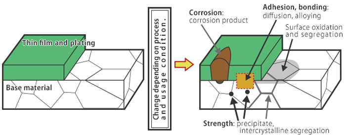
Material-dependent analysis techniques
The structure to exhibit the necessary physical property differs from material to material. We provide optimum analysis techniques according to the structure.
Physical Analyses based on Analysis Method
JFE-TEC observes and analyzes the sections, interface structures, and morphologies of products and composite materials that employ thin films and fine particles of metal, ceramics, and high polymers at nano-scale resolutions. We will also undertake precise sample preparation for observation of section/interface structure and morphology.
The size of controlled structure and analysis method vary from material to material.
We offer optimum analysis techniques for optimum morphological observation, element analysis, surface chemical state analysis, and crystalline structure analysis.
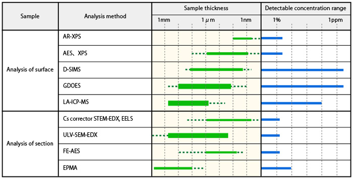
Practical sample thickness and detectable concentration range in nano material analysis
The practical sample thickness and detectable concentration range in various analysis methods are restricted. The table below shows some examples.
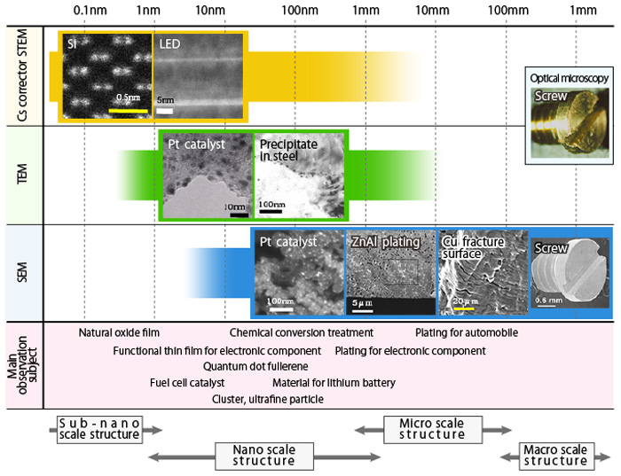
Selection of microscope for material
As the structure to analyze differs from subject to subject, the analysis method differs as well.
Main Evaluation Items and Analysis Methods of Physical Analysis (Our Proprietary Techniques)
Morphological observation
| Abbreviation | |
|---|---|
| Transmission Electron Microscopy with Cs corrector | Cs corrector TEM |
| Transmission Electron Microscopy | TEM |
| Ultra Low Voltage Scanning Electron Microscopy | ULV-SEM |
| Scanning Electron Microscopy | SEM |
| Focused Ion beam - Scanning Electron Microscopy | FIB-SEM |
Surface chemical state analysis
| Abbreviation | |
|---|---|
| X-ray Photoelectron Spectroscopy | XPS |
| Auger Electron Spectroscopy | AES |
| Secondary Ion Mass Spectrometry | SIMS |
| Time Of Flight-Secondary Ion Mass Spectrometry | TOF-SIMS |
| Electron Probe Micro-Analysis | EPMA |
| Field Emission-Electron Probe Micro-Analysis | FE-EPMA |
| Electron Energy Loss Spectroscopy | EELS |
| Thermal Desorption Spectroscopy | TDS |
| Raman Scattering Spectroscopy | RSS |
| Fourier Transform Infrared Absorption | FT-IR |
| Laser Ablation Inductively Coupled Plasma Mass Spectrometry | LA-ICP-MS |
Evaluation item: crystalline structure analysis
| Abbreviation | |
|---|---|
| X-ray Diffraction (capable of Rietveld analysis) | XRD |
| Electron Diffraction | ED |
| Electron Backscatter Diffraction Electron Backscatting Pattern |
EBSD/EBSP |
Evaluation item: composition analysis
| Abbreviation | |
|---|---|
| Inductively Coupled Plasma Atomic Emission Spectrometry | ICP-AES |
| Inductively Coupled Plasma Mass Spectrometry | ICP-MS |
| UV-VIS (Ultraviolet Visible Absorption Spectroscopy) - Spectrophotometer in near-infrared to near-ultraviolet region | UV-VIS |
| Atomic Absorption Spectrometry | AAS |
| Gas Chromatograph Mass Spectrometry | GC-MS |
| Liquid Chromatograph Mass Spectrometry | LC-MS |
Evaluation item: physical property evaluation
| Abbreviation | |
|---|---|
| Laser diffraction particle size distribution measurement | |
| Thermal Analysis | TA |
| Thermogravimetric Analysis | TG |
| Differential Thermal Analysis | DTA |
| Differential Scanning Calorimetry | DSC |
| Specific surface area measurement, pore size distribution (BET method) |
Evaluation item: working environment analysis/investigation
| Abbreviation | |
|---|---|
| Nano particle concentration measurement by TEM |
Example of Papers and Presentations at Symposium by JFE-TEC
| Paper/ symposium | Place of publication | Year of publication | Title |
|---|---|---|---|
| Paper | Journal of the Surface Finishing Society of Japan | 2013 | The Effect of Steel Sheet Pretreatment on Alloying Behavior of Galvanized Steel Sheet |
| Paper | Bulletin of Gunma Industrial Technology Center | 2013 | Forefront of Material Nano Structure Observation Using Electron Microscopy |
| International symposium | 6th International Symposium on Practical Surface Analysis |
2013 | "Damage of ZrO2 by Argon Ion Bombardment" |
| Domestic symposium | Polymer Material Meeting of The Japan Society for Analytical Chemistry | 2008 | New Analysis Method of Material Electrode Surface by Ultra Low Voltage SEM |
| Domestic symposium | 29th meeting held by Surface Analysis Society of Japan in 2009 | 2009 | Ultra Low Voltage SEM as New Form of Surface Observation |
| Domestic symposium | 1st Forum of Society for Study of Foreign Substances in 2009 | 2009 | Physical Analysis Technique for Foreign Substance Analysis and Malfunction Investigation |
| Domestic symposium | Meeting of the Surface Science Society of Japan in 2009 | 2009 | Progress of Material Observation by Ultra Low Acceleration Voltage SEM |
| Domestic symposium | Meeting held by Nanotech Department of The Surface Finishing Society of Japan | 2010 | Analysis Techniques in Nano Material Development |
| Domestic symposium | Meeting of the Surface Science Society of Japan in 2011 | 2011 | Roles of Surface Analysis in Progress of Steel Material |
| Domestic symposium | Meeting of the Japan Society for Heat Treatment in 2011 | 2011 | Forefront of Analysis of Metallic Material Microstructure by ULV-SEM |
| Domestic symposium | Meeting of the Japan Society for Applied Physics in 2012 | 2012 | Damage of Zr Oxide by Ar Ion Irradiation |
| Domestic symposium | Meeting of the Surface Science Society of Japan in 2012 32nd Surface Science Academic Meeting |
2012 | Damage of ZrO2 by Ar Ion Irradiation |
| Domestic symposium | Corporate exhibitions in 20th meeting held by Advanced Power Semiconductors Workshop, The Japan Society for Applied Physics | 2012 | Electron Microscopy Technologies Used According to Structure Size from Atomic Scale to Macro Scale |
| Domestic symposium | 37th conference of the Gunma Industrial Technology Center | 2013 | Forefront of Material Nano Structure Observation Using Electron Microscopy |
| Domestic symposium | Meeting of the Japanese Society of Microscopy in 2013 | 2013 | Examples of Utilization of Ultra Low-voltage Scanning Electron Microscopy for Surface/Interface Analysis |
| Domestic symposium | 22nd meeting of the Advanced Power Semiconductors Workshop, The Japan Society for Applied Physics | 2013 | Analysis of C State in Gate Oxide/SiC Interface Using Cs Corrector STEM |
| Domestic symposium | 22nd meeting of the Advanced Power Semiconductors Workshop, The Japan Society for Applied Physics | 2013 | Electron Microscopy Technologies Used According to Structure Size from Atomic Scale to Macro Scale |
| Domestic symposium | 30th panel discussion on rare earth by the Rare Earth Society of Japan | 2013 | Analysis Technique of Atomic Scale Structure of Intercrystalline Phase in Meodymium Magnet Using Cs Corrector STEM |
| Domestic symposium | 2nd meeting held by Advanced Power Semiconductors Division, the Japan Society for Applied Physics | 2014 | Techniques of Interface Observation Using Electron Microscopy According to Structure Size from Atomic Scale to Macro Scale |