Examples of Supported Analyses and Evaluations
TEM Observation of Li-Ion (Lithium-Ion) Battery Negative Electrode Material
TEM image
-
Example of TEM examination of the negative electrode material of a Li-ion (lithium-ion) battery
Sample: a Li battery receiving charge-discharge test that has been disassembled
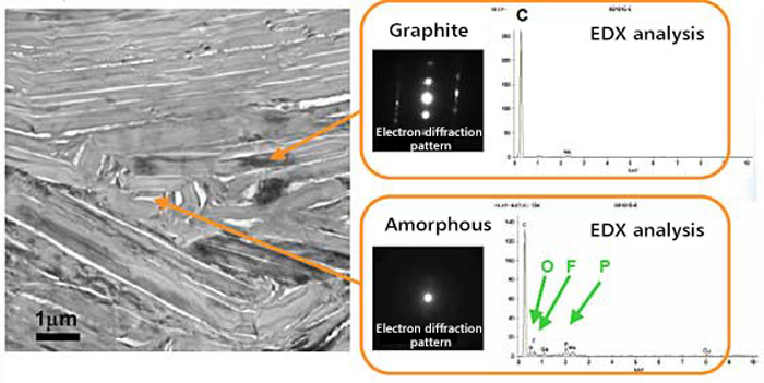
To evaluate the microstructure inside the negative electrode active material, it is effective to conduct TEM observation, EDX analysis and electron diffraction. The figure on the left is a cross-sectional TEM image of a particle of carbon used for negative electrodes. The slender layered part showing dark contrast is graphite, while the white part between the layers shows an area containing an electrolyte site. Active material and electrolyte are identified also from the electron diffraction pattern on the right and the result of EDX analysis.
Physical analysis for clarifying the microstructure (1) - TEM observation technique for nano-structure - 1: TEM image, electron diffraction -
Principle of the transmission electron microscope
The transmission electron microscope (TEM) is widely used as the most dominant means to evaluate the microstructure inside substance at an atomic level. TEM is capable of observing the microstructure of a thin sample with size approximately 100 nm or less by irradiating a highly accelerated electron (e.g., 200 kV) to the sample and magnifying the transmitted electron to form an image.
A TEM image generally reminds us of a bright field image. Its contrast results from Bragg diffraction of electron due to crystallization, atomic number, thickness of the sample, etc. TEM enables you to observe not only crystal grain, alloy phase, deposit and thin-film laminate, but also dislocation and stacking fault. In addition, for a dark field image formed only with a diffracted wave, it is capable of forming an image of only a certain crystal, and is therefore useful for checking the deposit and crystal grain size. Furthermore, it is capable of observing a lattice image if using the interference of the transmitted wave and diffracted wave.
Additionally, TEM enables you to grasp the crystalline state such as amorphous, single-crystal and polycrystalline, and determine the crystal structure, based on an electron diffraction pattern.
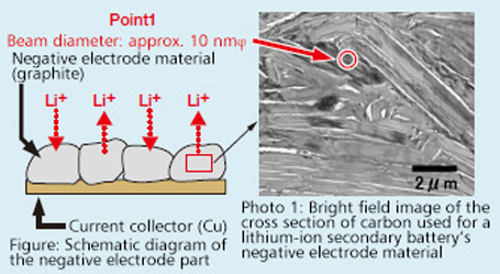
Example of observation using TEM
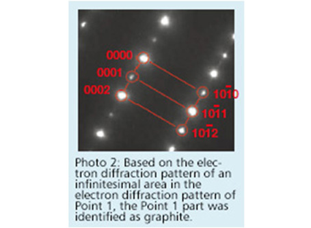
Photo 1 shows a cross-sectional TEM image (sample adjustment: based on FIB method) of a sliced carbon particle (tens of nm in thickness) of a lithium-ion secondary battery's negative electrode material. To prevent the battery performance from being deteriorated and secure safety of the battery, investigation using TEM has been actively conducted in recent years. The slender layered part showing dark contrast is graphite, while the white part between the layers shows an area containing an electrolyte site. Slight orientation, which is characteristics of natural graphite, is observed. Such orientation is said to contribute to the performance. Photo 2 shows an electron diffraction pattern obtained from an area with an electron beam irradiation diameter of 10 nm φ. The distance from the point in the center of the photo (0000) to the spots in the perimeter corresponds to the atomic spacing. The material can be identified as graphite by measuring the distance between the spots and performing calculation from the coefficient specific to TEM.
The nano world can be further clarified by mounting analysis equipment such as EDX or EELS to the TEM. These analyses will be described next time.