


Physical Analysis
Analysis Using FE-EPMA
(Field Emission-Electron Probe Micro-Analyser)
EPMA (Electron Probe Micro-Analysis) is a representative technique utilized in the evaluation, study, and quality management of various solid materials, such as metal, ceramics, and electron material. Among the physical analysis devices, the quantitative correction method has been established only in EPMA, and it has a power especially in determination in the minute area or welds that cannot be addressed by a wet method.
Due to FE (Field Emission) - EPMA equipped with a field emission type electron gun, it has been possible to analyze elements in a minute area of 100 nm in size, which had been impossible with conventional EPMA.
Measurement/Analysis Method
Overview
FE-EPMA enables element analysis in a minute area of approx. 100 nm in size. Also, using EDX, it is possible to analyze element combinations that are difficult to analyze since the peaks of elements overlap each other (Fe and F, Cr and O, Si, Ta and W, Mo and S) by separating them.
Quantitative evaluation of film thickness distribution in thin film is possible as well.
-
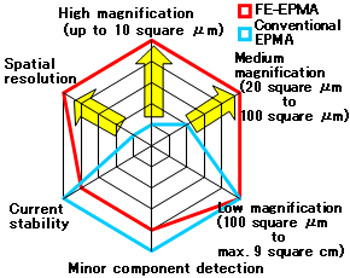
Features of FE-EPMA
-
Element qualitative analysis of minute area
Spatial resolution: 150 nm (370 nm conventionally) -
High-definition element mapping analysis
Maximum magnification: 20,000x (5,000x conventionally) -
High-sensitivity analysis
Analysis sensitivity: several hundred ppm (0.5% in SEM-EDX)
C quantitative analysis precision: 0.1% (unavailable in SEM-EDX) -
Applicable to almost all combinations from B to U(separation is impossible with SEM-EDX)
Analysis of combinations Cr and O, Fe and F, Mo and S, and Ag and Pd is possible. -
Analysis software with abundant functions
Phase distribution, particle size distribution, film thickness evaluation, determination of thin film, etc. -
Capable of handling large-size sample
Maximum size: 100 mm x 100 mm x 75 mm in height
-
Element qualitative analysis of minute area
-
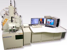
FE-EPMA (JXA 8500F from JEOL)
Example Cases of Analysis to which FE-EPMA can be Applied
| Field | Case |
|---|---|
| Battery | Analysis of electrode material in lithium-ion secondary battery (element mapping at section of positive electrode active material) |
| Electrics/electronics | Element mapping of Pb-free solder |
| Section observation of light-emitting diode | |
| Analysis of interface at solder welds (observation of interface diffusion to alloying) | |
| Section element mapping of capacitor | |
| Mapping of rare earth in display and fluorescent paint | |
| Section element mapping of electrode surface treatment layer | |
| Metal/steel | Mapping and particle analysis of precipitate and inclusion |
| Grain boundary evaluation of ferrite-based stainless steel | |
| Section mapping analysis of various plating layers | |
| Evaluation of decarburized layer and carburized layer | |
| Film thickness evaluation of functional thin film on metal | |
| Element mapping of oxide layer or rust layer of stainless steel and low alloy steel | |
| Highly functional magnetic material | Element distribution analysis by combination of FE-EPMA and EBSP |
| Others | Element mapping of ceramic-based material and alloy-based sintered material (evaluation of interface reaction with sintering aid) |
| Composition/film thickness distribution analysis of ceramic coating layer (CrN) | |
| Evaluation of morphology and distribution of catalyst metals including Pt and Ag-Pd |
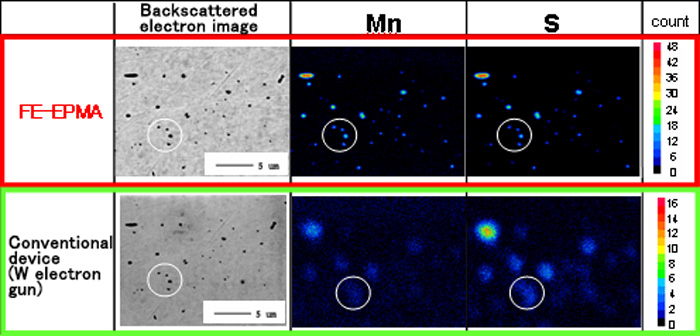
Analysis Case 1: Distribution of Fine Precipitates Dispersed in Pb-Free Free-Cutting Steel
|
The following is a case example where the element mappings were conducted in the same location under the same conditions by FE-EPMA and a conventional equipment (W-type EPMA). In mapping by FE-EPMA, as electron beams can be sufficiently narrowed even with a high current of 100 nA during analysis, it is possible to clearly identify the shape and size of fine precipitates of 1 μm or less in size. JFE-TEC is capable of proposing data analysis, including histograms and particle size distribution, using particle measurement software and phase analysis software according to the customer's needs. |
||
|
||
| Mn and S plane distribution in Pb-free free-cutting steel - comparison between FE-EPMA and conventional EPMA - (accelerating voltage: 10 kV, current value: 100 nA) |
Analysis Case 2: Concentration Distribution of Cr-Depleted Layer in Sensitized Stainless Steel
In ferrite-based stainless steel, the way Cr-depleted layer was produced near Cr carbide precipitated in the crystal grain boundary could be observed. The observation reveals the concentration difference by several percent in submicron areas.
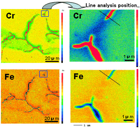
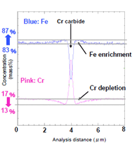
Cr and Fe concentration plane distribution and grain boundary line distribution in surface of sensitized ferrite-based stainless steel
(accelerating voltage: 10 kV, current value: 100 nA)
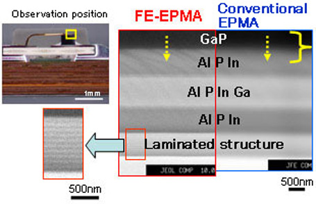
Analysis Case 3: Section Observation Case of Light-Emitting Diode Mounted on Cellular Phone
The following is a case example of SEM observation and line analysis by FE-EPMA and LaB6-type EPMA in the same condition. In FE-EPMA, the interface is clearly visible and fine multilayer structure of several tens of nanometers in size can be confirmed. If the spatial resolution is evaluated on the basis of interface between GaP and AlPIn, it has been enhanced 2.5 times from the conventional equipment.
-
Backscattered electron image (20,000X)
-
Distance from interface (nm)
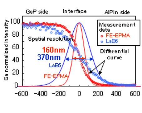
SEM photograph and Ga line distribution of section of light-emitting diode and interface resolution -
omparison between FE-EPMA and conventional EPMA - (accelerating voltage: 5 kV)
-
FE-EPMA Conventional EPMA Electron gun ZrO/W chip W, LabB6, CeB6 Accelerating voltage 3 - 25kV 10 - 25kV Minimum beam
diameterDuring observation 8 nm W 40 nm
LaB6 25 nmDuring analysis 0.1 μm W 0.5 μm
LaB6 0.3 μmMinimum plane analysis area 5 μm 30μm -
Related Links
- Battery-Materials Analysis & Evaluation
- Examples of Analysis of Rare Earth Magnet (Neodymium Magnet)
- FIB Equipped with Cryo-function that Alleviates Processing Damage
- EBSD Analysis Technique