


Physical Analysis
EBSD Analysis Technique
What is EBSD? It is an abbreviation of Electron Back Scatter Diffraction and also referred to as EBSP (Electron BackScattering Pattern). By using it in combination with SEM to manipulate electron beam and analyze pseudo-Kikuchi pattern, we measure microcrystalline orientation and crystal system.
Measurement/Analysis Method
Overview
Unlike X-ray diffraction by which average information can be acquired, this technique allows acquisition of crystalline particle-based information. Also, from crystalline orientation data, it is possible to analyze the orientation distribution of crystalline particle, which is aggregate structure, and the crystalline phase distribution.
Features
- By using SEM, it is possible to analyze crystalline structure.
- Due to measurement at a low accelerating voltage of 10 kV or less, EBSP analysis with a high spatial/depth resolution is possible.
- High-speed measurement has been made possible.
Information Acquired through EBSD Analysis Technique
Crystalline orientation analysis |
|
|---|---|
| Orientation mapping | Displays the orientations of crystalline particle with different colors. |
| Crystalline particle image | Displays crystalline particle (defined by arbitrary grain boundary inclination angle) |
| Crystal grain boundary image | Displays crystal grain boundary (by inclination angle, corresponding grain boundary, etc.) |
| Other analyses | Normal pole figure/reverse pole figure, orientation distribution function (ODF), misorientation dispersion function (MDF) |
Crystalline Phase Distribution Measurement |
|
| Phase distribution image | Displays difference in crystalline phase and area rate of phases |
Cases to which EBSD can be Applied
| Field | Case |
|---|---|
| Thin film/surface treatment |
Orientation measurement/structure observation of Al, Cu, Ni, Zn, Sn, alloy plating, etc. of thin film/plating (Al, Cu, Ni, Au, alloy layer, etc.) Observation of recording part of recording layer of optical disc |
| Bulk material |
Orientation analysis of crystalline particle of rolled texture, quenched structure and worked structure of steel material Distribution observation of residual austenite in steel material Orientation analysis, etc. of rolled/solidified structure of various metals Metal strain analysis |
| Highly-functional magnetic material |
Distribution of crystalline orientation in neodymium magnet Element distribution analysis by combination of FE-EPMA and EBSD |
| Joining/welding | Crystalline orientation measurement of silicon substrate for solar cell, metal welds (evaluation of coarsening of crystalline particle due to thermal influence),electromagnetic steel sheet, etc. |
EBSP of Oxide: Example of Chip Capacitor
-
BSE -
BaTiO3 
-
Phase map -
Ni 
By combining EBSP with ultra-low voltage SEM in low vacuum mode, EBSD measurement of insulated object is possible even without electric conductivity processing, and measurement of orientation distribution of oxide in capacitor is also possible.
Sample preparation: non-deposition, vacuum mode: 4 Pa, accelerating voltage: 20 kV, measurement range: 10 square µm in 0.02 µm steps
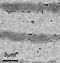
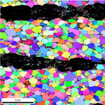
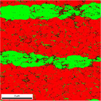
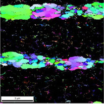
Analysis of Steel Material after the Fatigue Test: SEM Fracture Surface Observation/EBSD Strain Distribution
Surface Fracture Face Observation by SEM
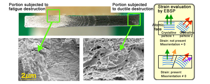
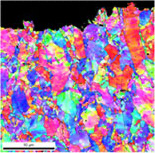
Section Orientation/Strain Distribution Analysis by EBSD
-
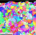
Orientation
distribution:
IPF map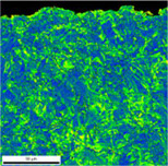
Strain
distribution:
KAM map -
Orientation
distribution:
IPF map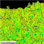
Strain
distribution:
KAM map
By using EBSD, it is possible to investigate the orientation distribution of crystalline particles as well as strain distribution.
- The KAM map reveals that at the portion subjected to ductile destruction, more strains are introduced compared to the portion subjected to fatigue destruction.
- The KAM map shows the misorientation between a certain measurement point and the adjacent portion, and the misorientation becomes large as the degree of strain increases and no misorientation occurs if there is no strain.
Measurement of Crystalline Orientation of Neodymium Magnet by EBSD
-
Secondary electron image -
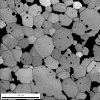
Image Quality image -
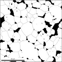
Crystal grain boundary image -
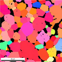
Nd2Fe14B
orientation distribution
-
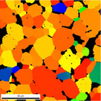
Image of angle distribution in
crystalline particle:
0° to 90° from (001)
-
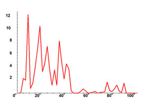
Histogram of crystalline
particle inclination angle
(angle from normal line)
By using EBSD, it is possible to investigate the orientation distribution of crystalline particles as well as their strain distribution.
- By conducting orientation measurement of main phase in 100 nm pitch, it is possible to conduct C-axis orientation measurement, grain boundary check and misorientation distribution measurement.
- The main phase is composed of crystalline particles of approx. 10 mm in size.
- In most of main phases, C-axis [001] plane is orientated. It is slightly inclined in the range of 0° to 40°.
Element Distribution Analysis by Combination of FE-EPMA and EBSD
Dy FE-EPMA mapping
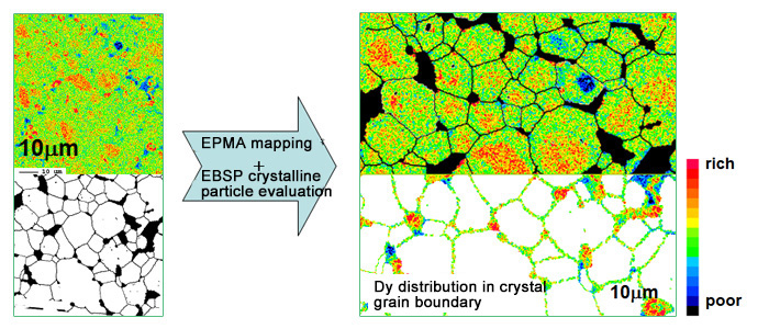
EBSP: Crystal Grain Boundary Image
Overlapping of a crystal grain boundary image (grain map) over EPMA mapping reveals that Dy exists inside particle and in grain boundary.
In this manner, we also propose a composite analysis method in which respective advantages of EBSD and FE-EPMA are utilized.
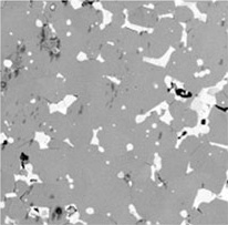
Distribution of residual austenite in steel: EBSD phase distribution image
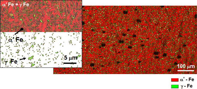
As a wide range is measured at 100-nm resolution:
It is possible to obtain the distribution of submicron-size residual austenite phase (g-Fe phase) in a mm-order range.
Basic Specifications of Ultra Low Voltage SEM-EBSD
| SEM main body | Ultra 55 from Carl Zeiss
Accelerating voltage: 100 V to 30 kV Resolution: 1.0 nm@15 kV, 1.7 nm@1 kV, 4.0 nm@100 V |
|---|---|
| EBSD analysis | Hikari High Speed EBSD Detector from TSLSoftware OIMTM Ver 5.2 |
| Analysis function | EDX: NSS300 from Thermo Electron |
Lineup of our EBSD analysis devices
| EBSP model | SEM model | Electron gun model | Minimum analysis area | Feature |
|---|---|---|---|---|
| Hikari High Speed EBSD Detector from TSL |
SUPRA VP40 from Zeiss | Shot key FE | <0.1μmφ | New introduction: ultra high sensitivity, high resolution, high speed |
| Digiview IV from TSL, OIM System Ver.6.2 |
FE-SEM JSM-7100F from JEOL |
Shot key FE | <0.1μmφ | High resolution, transmission EBSP, wide range EBSP, supporting non-exposure to atmosphere |
| From TSL | FE-SEM JSM-7001FA from JEOL |
Shot key FE | <0.1μmφ | High resolution |
| From TSL | JSM-840F from JEOL | Cold FE | 0.5μmφ | High resolution |
| Other general-purpose SEM-EBSD: two models | ||||